Stories of Manufacturing#06
GaN paves the way to
carbon neutralityDeveloping next-generation
GaN power semiconductor devices
GaN Device Development Enters a New Stage
December 2023 - The awards ceremony for the ‘”Ultra’’ Manufacturing Components Award was held in Tokyo.
The award is sponsored by Monozukuri Nippon Kaigi and Nikkan Kogyo Shimbun. 2023 marks the 20th year of the award, targeting components and materials that contribute to enhancing the competitiveness of Japan’s manufacturing industry as well as the development of both industry and society.
ROHM's EcoGaN™, a GaN device that significantly contributes to greater application energy-savings and miniaturization, received the ‘Electrical/Electronic Component Award’, one of six product awards.
From early on, ROHM has been involved in the development of GaN devices, which have been attracting attention worldwide in recent years. This recognition of ROHM’s technological expertise and product development strategy is not only welcome news for members of the Power Stage Product Development Department, which is still in its early stage of business, but was also a signal that the research and development carried out over many years had finally entered the next stage.
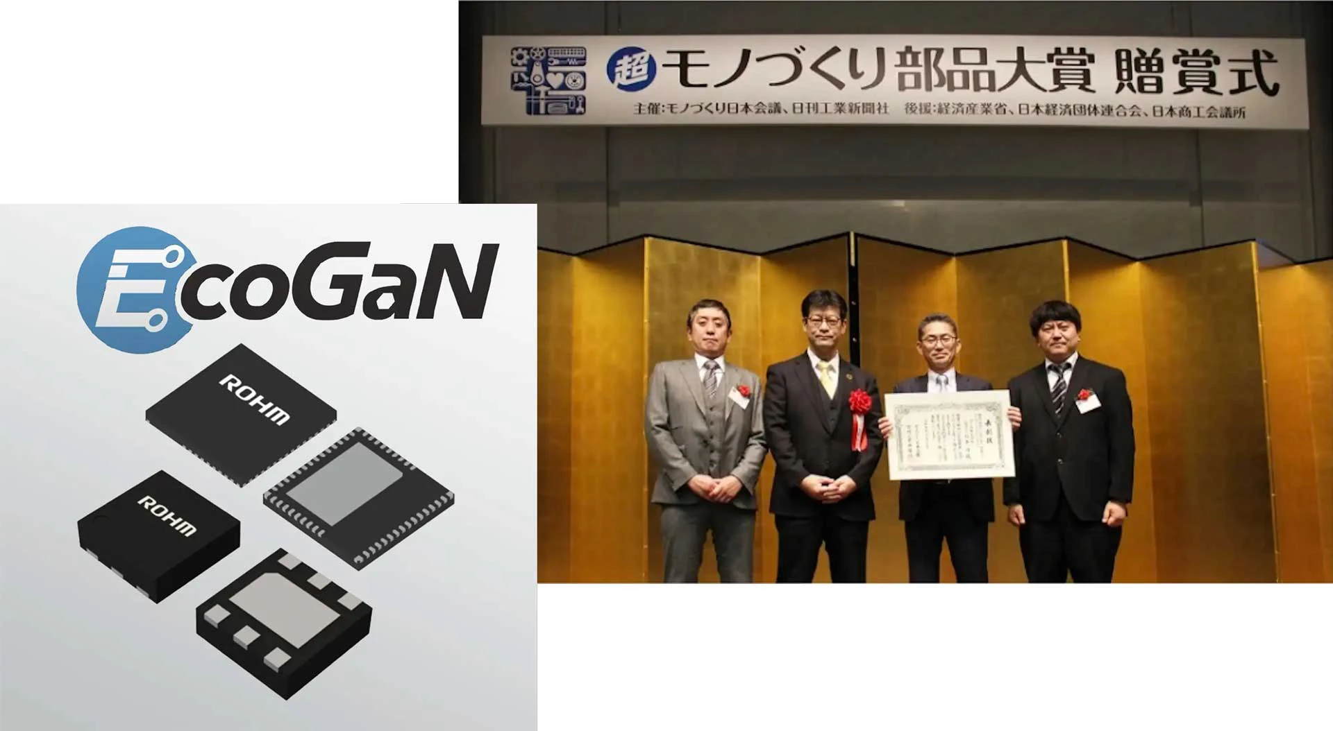
At the ‘”Ultra” Manufacturing Component Awards’ Ceremony ▲
◀▲ EcoGaN™ Series Products
Top: GaN HEMT Power Stage IC Bottom: GaN Gate Driver IC
Prompted by Customer Feedback
The award was given in recognition of not only the GaN device itself, but also the entire product line, including gate driver ICs that maximize the performance of GaN.
According to Mr. Otake, who has been involved with GaN development for more than 15 years since the era of pioneering research, ‘This speaks to GaN’s position as a next-generation device.’

Power Stage Product Design Division. LSI Business Unit Manager
Hirotaka Otake
I had focused on the light-emitting properties of GaN since I was a student. Then after joining ROHM, worked on both GaN and SiC power devices. The extensive experience gained in the research and development of devices, packaging, and applications proved to be very useful in launching new businesses.
Surprisingly, when listening to customers who were not ready to adopt GaN, many expressed expectations related to ease of use, involving control-side drivers, package types, and even modularization that incorporates driver ICs.
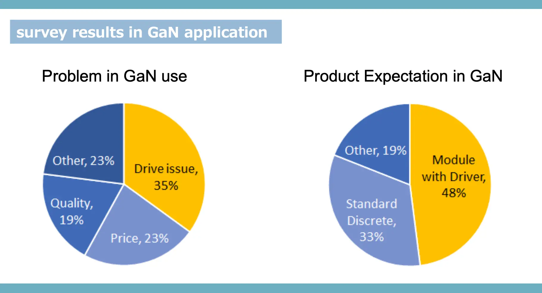
The results of customer feedback from the field indicate a clear demand for
・ Addressing drive-related challenges/modularization that includes driver ICs
Otake:
‘It's true that GaN devices are extremely difficult to handle, especially in terms of driving. This sentiment has become somewhat of a consensus within the industry. Although the switching characteristics of GaN at high frequencies are a huge advantage, there is a limit to what can be achieved by focusing solely on the characteristics of power devices to stably control power sources in the 1MHz range and beyond.
So by taking a slightly different approach, a new direction emerged, one that integrates the power device and driver IC in a single package. Otherwise, there may never be products that customers feel comfortable using, right? In other words, we started thinking that maybe the GaN market may never fully materialize.’
ROHM’s Unique Approach
Otake:
‘From this viewpoint, it’s undeniable that ROHM's abundant resources have been a boost in restarting development.’
You could say that our track record and pride in continuing to produce analog ICs that respond to the needs of the times for more than half a century have inspired and ignited the spirit of our engineers. In the power supply IC field where ROHM excels, we have cultivated wide ranging development knowledge and expertise, along with the personnel and facilities capable of ensuring quality in mass production.
At the same time, we also possess significant advantages regarding GaN devices. Namely production expertise developed early on for mass producing blue GaN LEDs at ROHM Hamamatsu.
In the development process, where achieving high quality stable mass production of GaN crystals is crucial, being able to establish a development base right next to the LED manufacturing line was an invaluable driving force, he says.
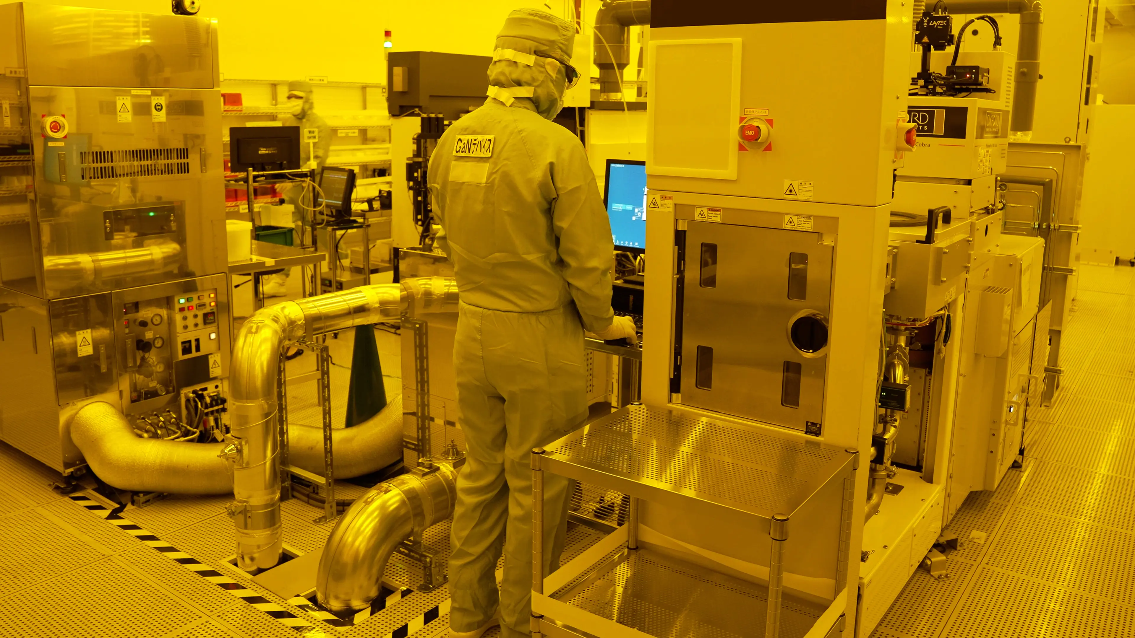
ROHM Hamamatsu GaN manufacturing line
・ Manufacturing line that supports mass production of GaN wafers The technology for growing stable thin film crystals on silicon substrates is key
A new project was launched to commercialize both power supplies and ICs, bringing together engineers with expertise and knowledge in different technologies. Full-scale development accelerated as we entered the 2020s.
Otake:
‘Initially, it started out as an internal venture, so the number of engineers and facilities involved was small, and we had to obtain company approval every year (chuckles), but when it came time to implement what we had built up, our unique strengths as a comprehensive manufacturer certainly accelerated the development process.’
Towards achieving a sustainable society
Here, let’s summarize the expectations for GaN devices along with their characteristics. The figure below is a distribution of applications mapped on the power/frequency axis, showing the dominant area of each power device. Unlike SiC power devices, which have shown increasing promise in recent years for switching in the high-power range, GaN is strong in applications requiring high-frequency operation in the MHz band.
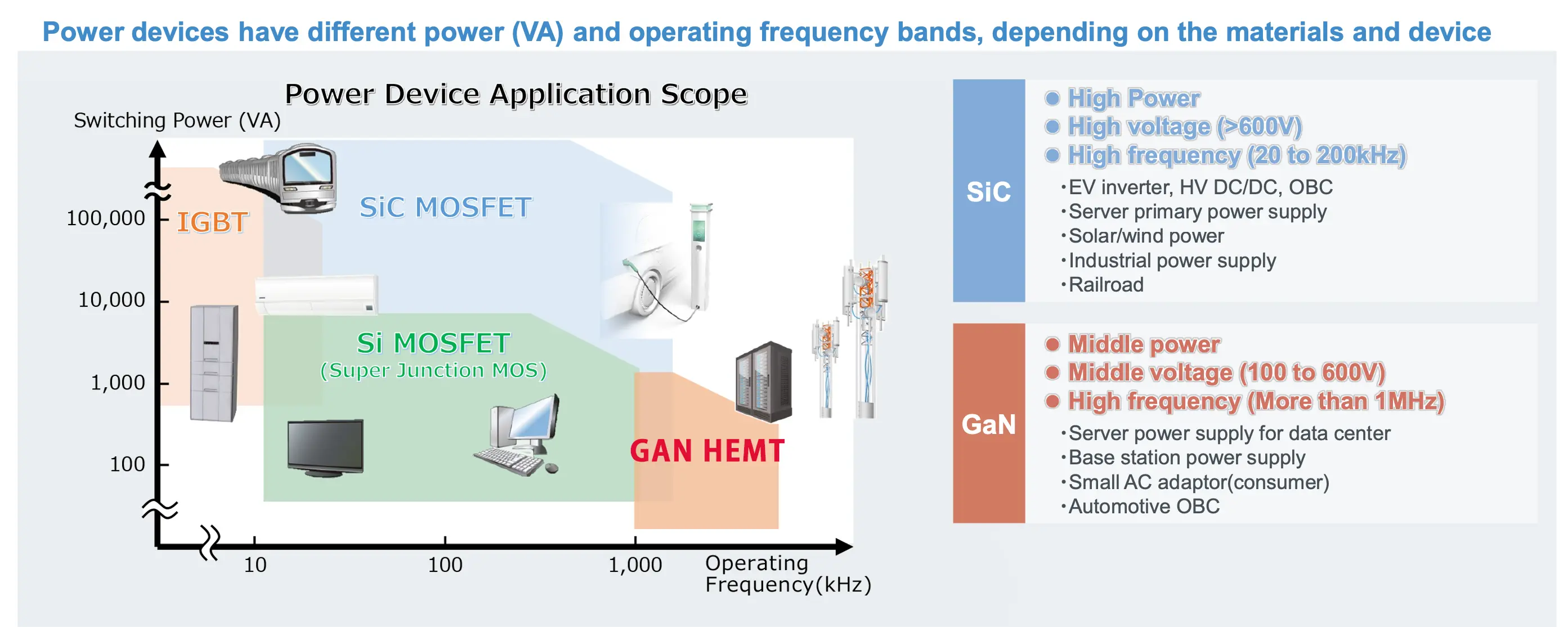
Target Applications
・ GaN is expected to be adopted in medium power high frequency applications
One is improving switching efficiency in the high frequency range above the MHz band. Another important feature is the ability to significantly contribute to set miniaturization.
At this time, the areas where the highest demand is anticipated are the consumer sector, such as fast chargers, and data centers in the telecommunications field. More specifically, power consumption in the telecommunications sector is already estimated to account for 3-5% of the world’s total electricity consumption, and with the increasing number of servers for deep learning utilizing AI-equipped devices together with the advent of the era of Afull-scale autonomous driving, the communication volume is expected to increase by as much as 100- to 1000-fold.

Otake:
‘ROHM’s corporate statement is “Electronics for the Future,” signifying the company’s commitment to solving societal issues through electronics. Facing the significant goals of reducing power consumption and achieving carbon neutrality, we are always thinking about how much our technologies can contribute. This serves as the driving force behind our daily efforts.'
From saving power in social infrastructure to reducing the size and weight of AC adapters, and even extending the flight range of drones, our goal is to provide the value of GaN to customers in a variety of fields not limited to specific applications. To this end, he says that the key phrase is to focus on creating 'GaN products that are easy to use.
At the same time, we asked Mr. Gunji, the engineer in charge, about the ‘difficulty in handling’ GaN from the viewpoint of device development.
Challenging the Gate Breakdown Barrier
Gunji:
'An important feature of GaN is high frequency operation, but as frequency increases signals become faster.
These signals are received by the GaN gate terminal, which is prone to instability at high speeds. The ‘difficulty’ in handling GaN lies in its tendency to break down even during minor voltage spikes.'
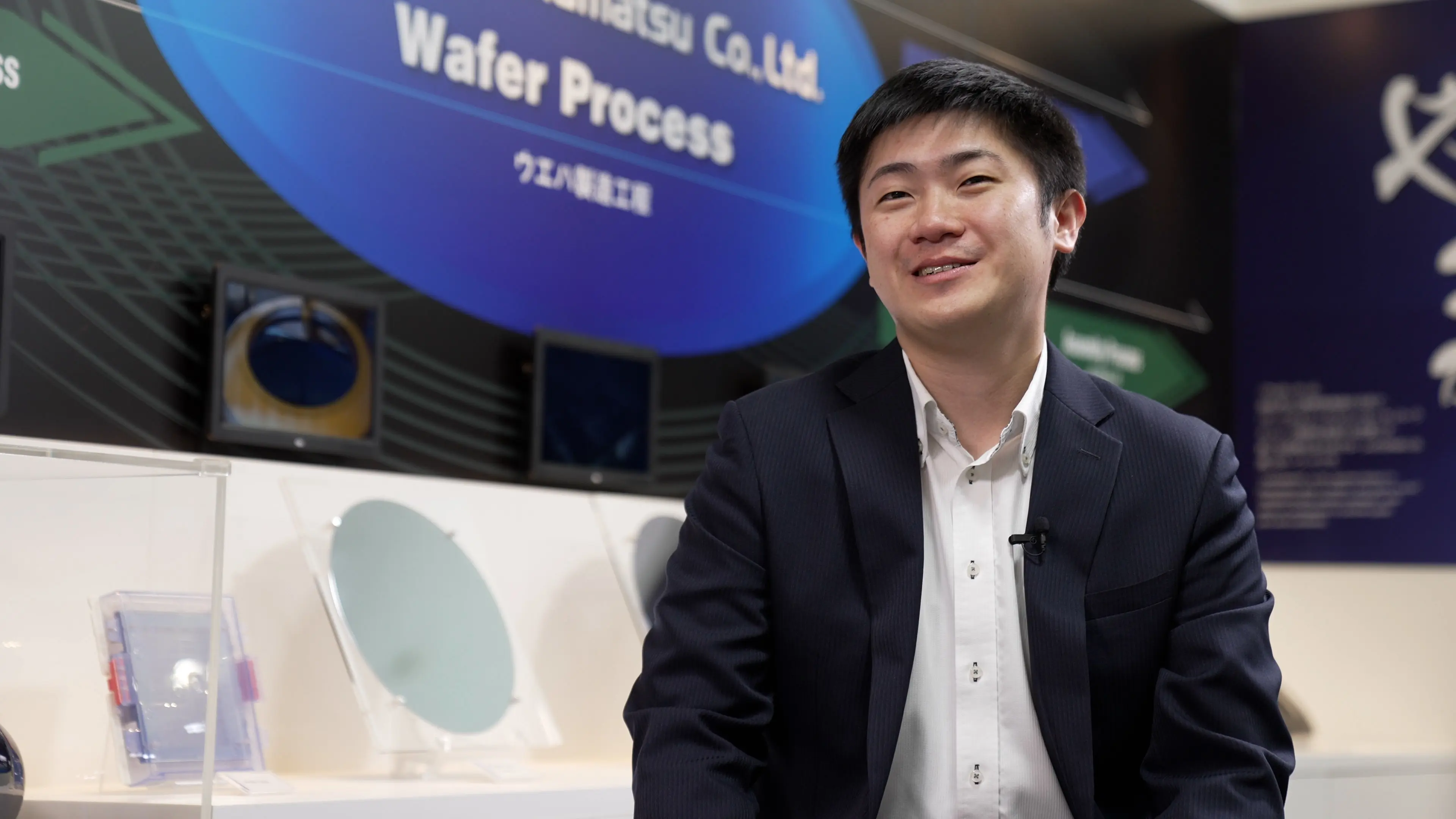
Manufacturing Engineering Department.
Power Stage Product Design Division. LSI Business Unit Engineer
Yoshikazu Gunji
A young engineer whose hobby is visiting the top 100 castles in Japan, he feels a great sense of accomplishment in being able to challenge the global GaN market while incorporating proprietary technology.
As a countermeasure, there have been cases where gate resistors were added to the intermediate circuit to avoid overshoot, but this has a side effect of slowing down the switching speed, leading to repeated trial and error to avoid reducing the advantage over silicon devices.
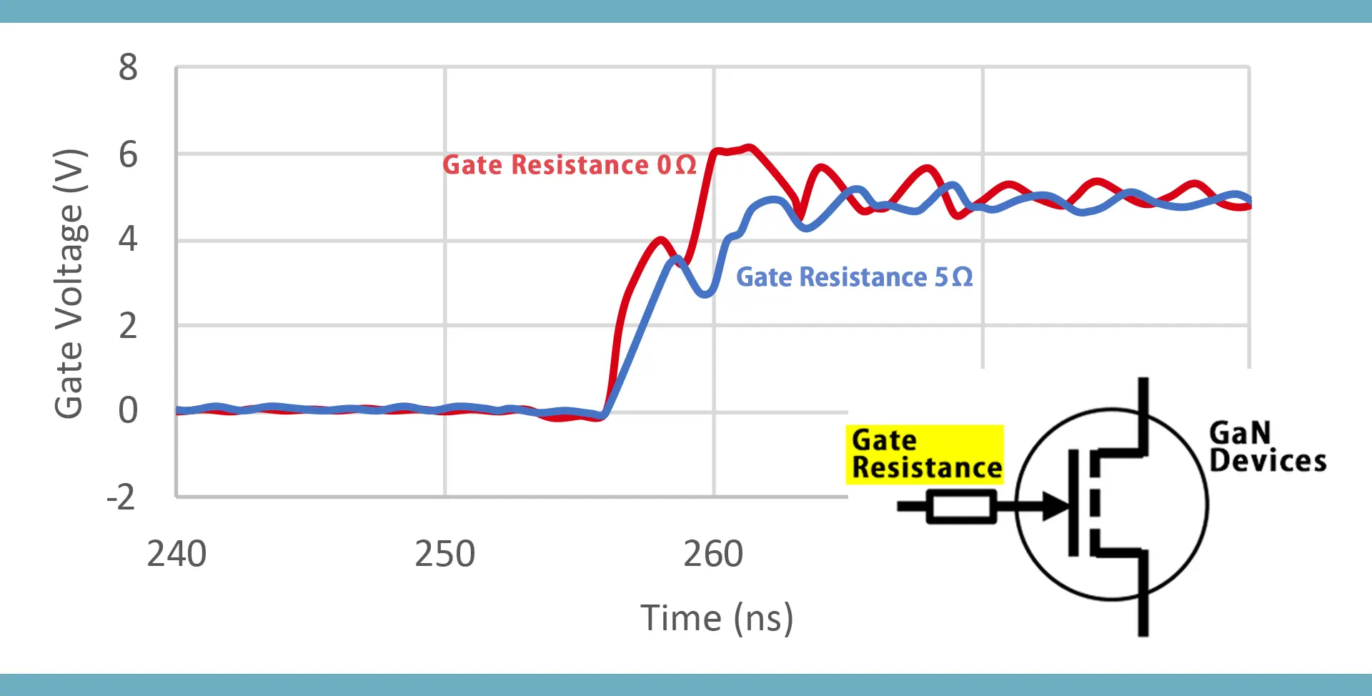
Gate resistor (5Ω) adoption case
・ Red graph/overshoot occurs
・ Blue graph/Overshoot avoided but rise time is slow
There is an option of controlling overshoot internally by creating a module that includes a gate driver IC, which ROHM is concurrently developing, but it is also important to meet the demand for discrete components
How strong of a gate can be made... To meet and overcome this challenge head-on, it was necessary to make drastic changes to not only the semiconductor itself, but also to the manufacturing equipment.
Gunji:
‘We were inspired by the characteristics of a failed structure that was accidentally created during the development process, then considered how to make it stable. Needless to say that we had to balance performance and quality along with productivity, which proved quite challenging.’
The graph below illustrates the performance of <Strong GaN> (achieved after around two years of trial and error) compared to existing products.
Under the 5V drive standard, conventional GaN has a voltage margin of only about 1V, causing damage during overshoot. In contrast, ROHM’s newly developed gate source voltage technology supports voltages up to 8V. High reliability is ensured by providing 3x the voltage margin of previous models.
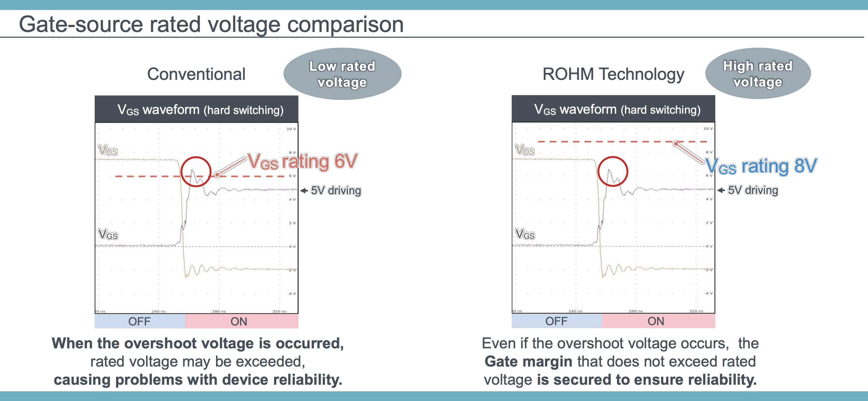
Comparison of ROHM’s new technology (right) vs conventional products (left)
・ The difference in the margin region for voltages above 6V significantly impacts the usability of GaN devices
Dedicated GaN Gate Drivers
While the devices themselves are evolving toward GaN that is easier for customers to use, there have also been technological breakthroughs in the gate driver ICs that drive GaN. One solution that ROHM has come up with in the analog IC field is the development of a GaN-specific gate driver IC.
Shinozaki:
‘In reality, there aren't many dedicated GaN gate driver products on the market just yet. Our mission was to maximize the performance of GaN without worrying about overshoot and other risks inherent with GaN. As an engineer, the incredible potential of this material that far exceeds silicon has definitely sparked my interest.’

Power Supply Product Design Department.
Power Stage Product Design Division. LSI Business Unit Group Leader
Yuichi Shinozaki
He is an unconventional(?) engineer proficient in judo at the third dan level, befitting his fearless appearance. His current department, comprised of people from different fields and professions, is filled with various stimuli that has broadened his perspective and values.
These insights were shared by Mr. Shinozaki, who joined the Power Stage Product Development Department as an IC design engineer. He remains highly motivated by the opportunity to put his considerable power supply IC development experience to use on this project.
The key phrase in this development is ‘speed in the nanosecond (ns) range.’
Overshoot is suppressed by adopting two special circuits. This enables ultra-fast switching with a minimum gate input pulse width of 1.25ns, maximizing the capabilities of GaN in applications.
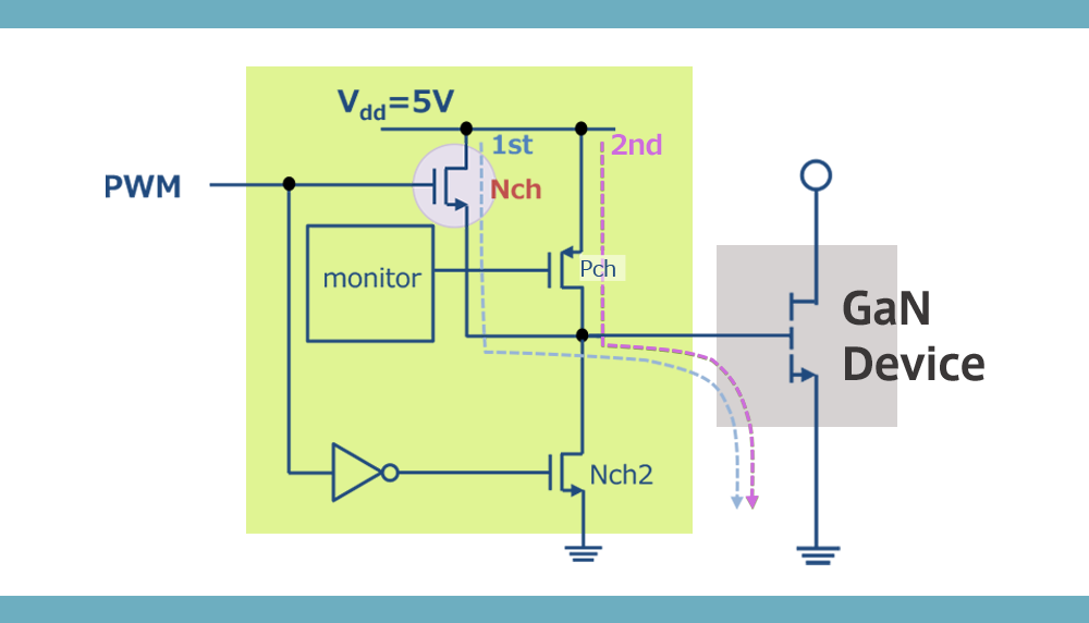
GaN gate driver IC circuit diagram
・ Special drive circuit to suppress overshoot beyond 6V and a bootstrap circuit unaffected by the reverse characteristics of GaN
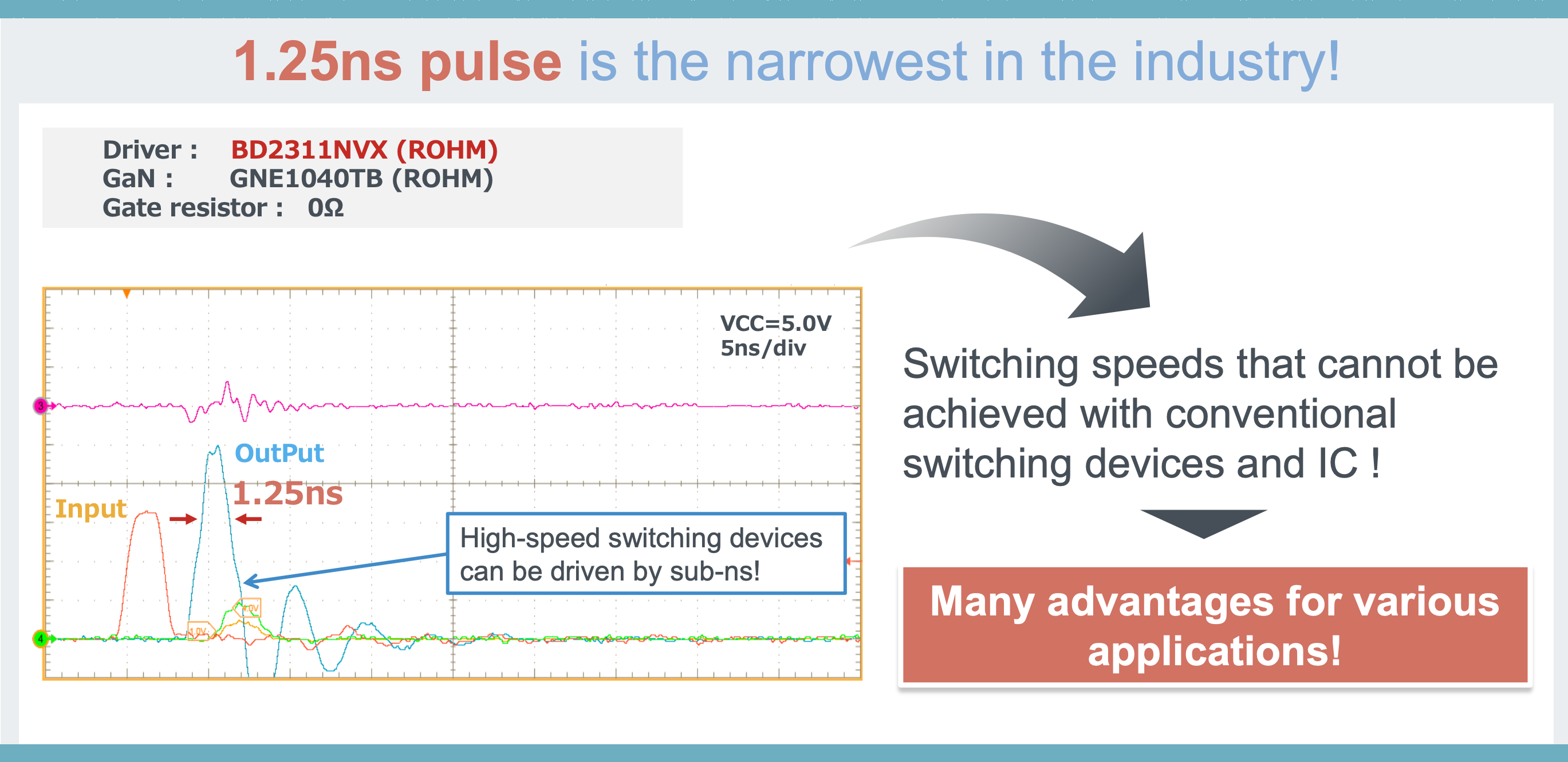
Pulse width = 1.25ns = industry-best
Nano Pulse Control™ and System-in-Package
In addition, as the control circuit side also needs to support higher frequencies, ROHM's original power supply technology Nano Pulse Control™ is used as the cornerstone. One of three Nano power supply technologies released in 2017, this was developed by leveraging proprietary analog expertise that allow us to propose power supply solutions for applications requiring higher voltages and frequencies.
Related Link(s)
ROHM’s innovative ‘Nano’ power technologies achieve breakthrough energy savings and miniaturization
https://www.rohm.com/support/nano
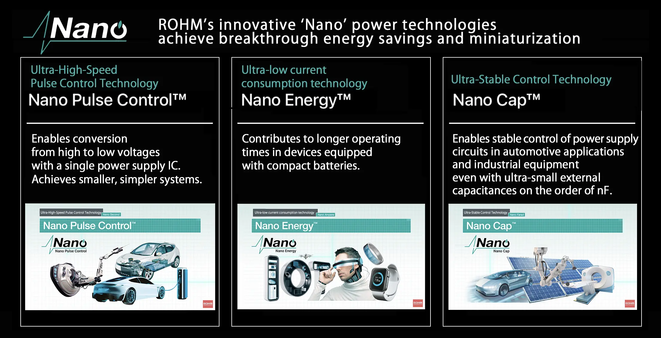
The Nano series consists of three cutting-edge power supply technologies
・ Nano Pulse Control™ on the left side of the figure above is used for GaN
Ando:
‘When Nano Pulse™ was first released, it featured the world’s smallest pulse width of 9ns, but this has since been improved to between just 1-2ns. Nano Pulse™ technology has been developed and evolved mainly for applications/markets requiring step down from 48V power supplies. This achieves with a single chip what conventionally requires two chips (stages) for DC/DC step-down conversion, dramatically reducing set size and power consumption.
We are confident that combining this technology with GaN will allow us to meet a wide range of customer needs in areas that were previously unattainable with silicon’
Mr. Ando, who like Mr. Shinohara who was recruited to the Power Stage Product Development Dept., mentions that he wants to develop products that further maximize the potential of Nano Pulse Control™ technology by combining with GaN.

System Power Supply Product Design Department.
Power Stage Product Design Division. LSI Business Unit Senior Engineer
Hiroaki Ando
He is a seasoned veteran of the the industry who has been developing power supply ICs across various departments for over a quarter of a century. While working to improve energy efficiency each day, it appears that he is also focusing on < Nano Energy™ >, a part of the < Nano Power Supply > series.
Ando:
‘We believe that the advantage of reducing the converter circuit from two stages to one will pave the way for a single-package solution that bundles the GaN device, gate driver, and controller IC which serves as the ultra-high-speed control tower.’
Ando states that the controller IC utilizing Nano Pulse Control™ has already reached the level of commercialization. The company is now working at full throttle to develop an all-in-one product for the future.
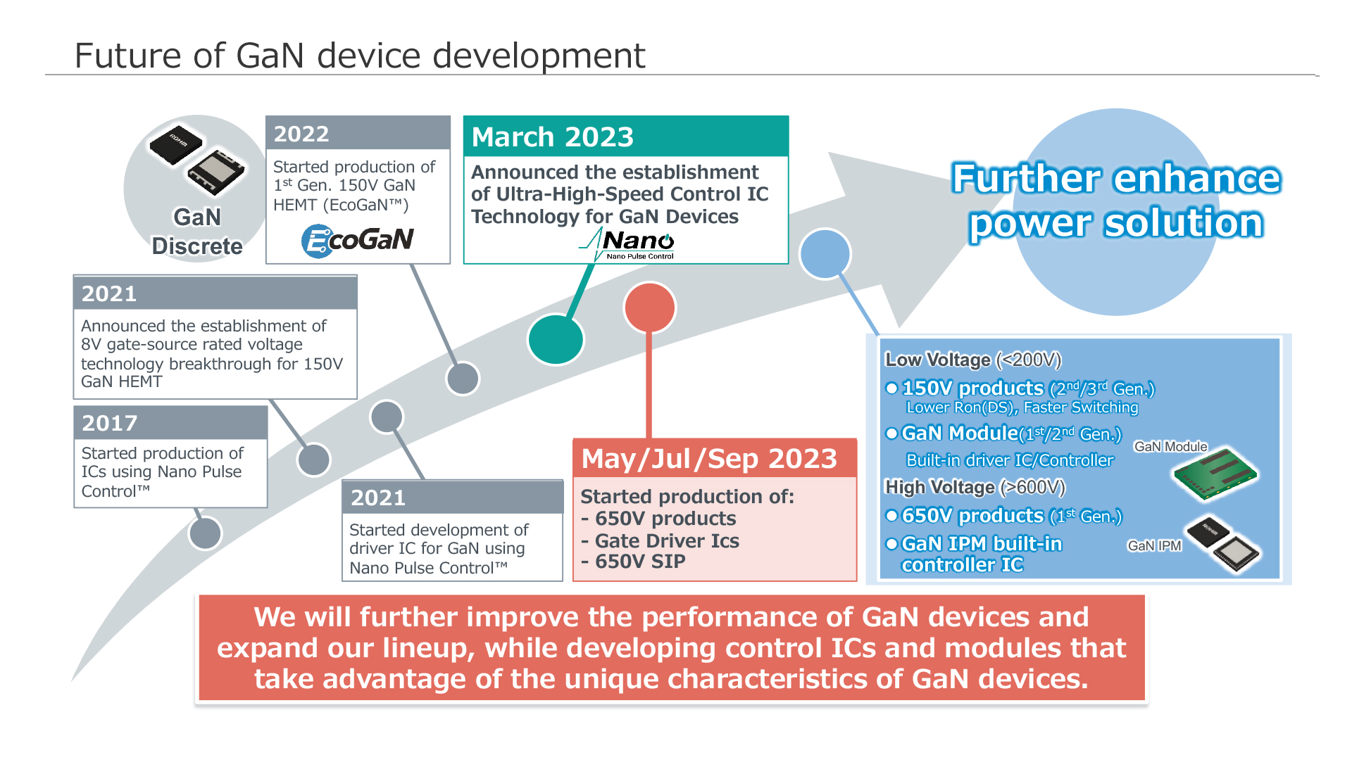
EcoGaN Series Development Roadmap (as of 2024)
Otake:
‘We started mass production of EcoGaN™ products in 2022, but this is just the first step for us. By proposing products that accurately meet the current and future needs of customers, we hope to slowly build up trust. Our mission is to steadily increase the number of GaN power stage ICs that provide superior performance and are easy for customers to use.’

GaN evaluation boards tailored to each application
・ In addition to proposing GaN products to customers, we offer evaluation boards that support development by facilitating product evaluation
The GaN device market is expected to become increasingly active as major overseas manufacturers are announcing their entry. However, there remains little doubt that ROHM will demonstrate its considerable expertise as a manufacturer capable of maximizing the performance of GaN from both the device and IC sides.
The evolution of GaN as the third pillar following silicon and SiC has finally entered a new stage.
Related Link(s)
GaN Power Devices
https://www.rohm.com/products/gan-power-devices


Otake:
‘ROHM had been working on GaN-R&D as a 3rd strategic material followed by Si and SiC, but things did not go as smoothly as we had hoped. And to be honest, there was a time in the late 2010’s when we almost gave up. At the time, we collected feedback from customers, which pointed us in a slightly different direction.’